E-MRS: perfect materials as the base for technical innovation
Professor Peter J Wellmann, President of the European Materials Research Society, discusses ‘perfect crystals’ and relates the European Materials Research Society’s focus areas to the five missions outlined in the European Council’s current programme.
The phrase ‘perfect materials’ needs a further specification in order to use it in a scientific and technologic context. ‘Perfect’ can be related to the perfect ordering of the atoms, high purity, the maintenance of a defined composition, or even the precise fulfillment of a certain specification. The latter could even be related to a necessary disorder which, by itself, would be the basis of a certain functionality. Looking at the tremendous technologic development through solid state electronics that has enabled today’s computer and communication technology, the term ‘perfect materials’ is closely related to an undistorted ordering in solid semiconductor materials that in addition exhibit the highest possible purity. To come to the point: almost all performance devices and applications make use of perfect crystalline materials.
Within materials science, the discipline of ‘crystal growth’ was able to provide Si boules exhibiting a perfect atomic order. From the materials point of view, the semiconductor silicon (Si) is the basis of all kinds of solid-state switches and integrated circuits implemented. Today’s electronics and computer technology would be unimaginable without these exceptional semiconductor crystals. An additional key application of silicon is photovoltaics.
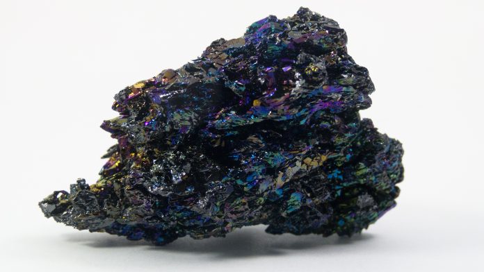
Silicon carbide (SiC), which is basically a blend of Si and diamond, is now in the process of taking over the place of Si in power
SiC as the new semiconductor for energy saving applications
Another semiconductor, silicon carbide (SiC), which is basically a blend of Si and diamond, is now in the process of taking over the place of Si in power electronic applications. Despite the advances in Si processing technology having not yet reached SiC technology, the extraordinary physical properties of SiC compared to its counterpart Si have raised SiC to the status of the new star material in power electronics. Due to the 10-fold break down field and three-fold heat conductivity compared to Si, the usage of SiC enables much lower electrical switching losses and much greater device operation robustness.
In the medium-voltage range between 600 V and 1.7 kV, applications like photovoltaic inverters, electrical motor control units, (hybrid) electrical vehicles, and uninterruptable power supplies profit from the physical properties of SiC. In the high-voltage range above 1.7 kV, wind energy, rail transportation, and smart power grid applications significantly benefit from SiC power electronic devices. SiC devices also have greater high voltage robustness, lower power consumption, and improved heat dissipation compared to their Si counterpart.
In a more general view, green energy concepts significantly depend on the provision of electrical energy using photovoltaics and wind energy, and smart electrical grids are needed to distribute that energy. From an industrial perspective, it is no longer the question whether SiC will replace Si in power electronics, but rather the question is how fast SiC wafer and device production can be ramped up to cover the constantly increasing demand.
Within the crystal growth lab of the University Erlangen-Nürnberg (FAU, Germany), R&D focuses on the growth and characterisation of SiC crystals and thin films. The lab is listed by the European Union as a Key Enabling Technology (KET) Centre on ‘FAU – Industrial Services in Crystal Growth of SiC’. In this context, technologic developments are transferred to industry in several bilateral agreements. Recently, the German Science Foundation approved a project to further develop the in-situ visualisation of the growth of large area SiC boules using 3D X-ray based computed tomography (CT). This project is carried out in a joint activity of the crystal growth lab at FAU with the Development Center X-ray Technology EZRT of the Fraunhofer Institute. With the upscaling of the in-situ CT system, growth process-related phenomena of 150mm and 200mm SiC boules will be investigated, which represent the current state-of-the art as well as the upcoming SiC wafer sizes in industrial production, respectively.
A major part of the R&D efforts is related to the hexagonal, so-called ‘4H-SiC’ polytype that is applied in power electronics. Another polytype of SiC of emerging interest is the cubic, so-called ‘3C-SiC’ polytype. The processing of 3C-SiC semiconductor wafers has been found to be much more difficult than that of standard hexagonal material. Nevertheless, the crystal growth lab is participating in two Horizon 2020 projects – CHALLENGE (2017-2021) and SIComb (2020-2023) – which focus on bulk materials and thin films of 3C-SiC, respectively.
A large number of projects related to technology transfer are carried out with direct funding from industry. The technological innovation is enabled by fundamental materials studies. This is the base where the materials platform, as it is provided by the European Materials Research Society, plays a key role. The scientific research is strongly fostered by a vivid exchange with experts looking at the discrete problems in an interdisciplinary context.
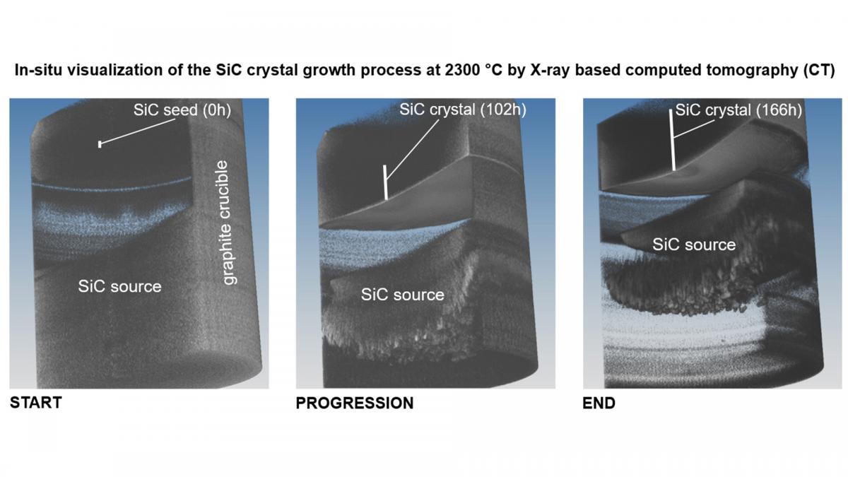 |
| In-situ visualisation of the SiC crystal growth process at 2300°C by X-ray based computed tomography (CT). Presented at the E-MRS 2019 spring meeting in Nice (symposium X, silicon carbide & related materials for energy saving applications) |
Green energy and novel materials
With the progression of ‘green’ power stations, the issue of the short-, mid-, and long-term storage of electrical energy comes to the fore. It is believed that the production of ‘green’ hydrogen using electricity from photovoltaics and wind energy will play a major role in developing the field of energy storage. Innovative solutions are necessary to solve this tremendous challenge. Looking at the aforementioned material SiC from a much broader perspective, it turns out that p-type doped SiC offers superior properties when it comes to the photocatalytic splitting of water into hydrogen and oxygen. Such photoelectrochemical cells combine the classic solar cell and hydrolyser in one unit.
In addition to SiC, there are many other materials being discussed by the scientific community that could be applied in this way. It is again the European Materials Research Society that plays a key role in bringing together experts from all over the world to discuss their new findings.

© iStock/nd3000
The bigger European and global view on functional materials
Since the early 1980s, the European Materials Research Society has been serving the scientific and engineering community by bringing together experts from physics, chemistry, biology, medicine/pharmacy, and engineering in general. Founded in 1983, the European Materials Research Society was the first such society in Europe and is now the largest, with over 4,000 members from industry, government, academia, and research laboratories, who meet on a regular base to share recent progress in functional materials science.
Although the majority of European Materials Research Society members are from countries in the European Union, European Materials Research Society is and has always served the scientific community in all European countries. In 2021, as a result of the COVID-19 pandemic, the European Materials Research Society meetings will be carried out as virtual or hybrid meetings.
In a more general sense, ‘perfect materials’ are not limited to semiconductors. However, in essentially every area of daily life, new and old materials with significantly improved performance play an important role. Therefore, European Materials Research Society has recently defined six topical areas which will be fostered in the coming years:
- Bio and nanomedical materials;
- Materials for sensing and embedded systems;
- Advanced battery materials and processing/energy storage materials (including green algae);
- Materials for quantum information;
- Materials and processes for additive manufacturing; and
- Resources, recycling, and sustainable material development.
In a cross-disciplinary action, European Materials Research Society pursues education in the field of ‘Artificial Intelligence (AI) in materials science research’. It is believed that the concepts of big data, machine learning, and artificial intelligence are providing new tools to search for new materials and to develop advanced processes.
These topical areas fit very well into the five missions that have been identified by the European Council as strategic topics for the coming years:
- Adaptation to climate change including societal transformation;
- Cancer;
- Healthy oceans, seas, coastal and inland waters;
- Climate-neutral and smart cities; and
- Soil health and food.
These five topical areas have been formulated from the point of view of the societal challenges facing not only Europe but also the wider world.
Within these missions, in almost every case materials are the base for the devices, which themselves are part of the application solution. For example, semiconductors may be used in sensors in order to detect the composition of air or to measure the ambient temperature. In fact, gas and temperature sensors are of importance for all five missions: They may be used to monitor changes in climate; they are important for diagnosis of diseases; they are necessary to determine the conditions of our environment; they are inevitable to control air conditioning systems; and they can detect the status of farmland.
The role of the European Materials Research Society in this context is to bring together experts from interdisciplinary fields to identify solutions for various problems. European Materials Research Society’s first task is to provide the platform for scientific and technology-driven dialogue between experts from specific fields. The equivalent second task is to initiate an interdisciplinary exchange. European Materials Research Society aims to help experts from science and technology to bring their ideas and solutions to serve the needs of society, such as those that are enumerated in the five missions mentioned above.
For this reason, European Materials Research Society sees itself as a European platform with strong links to a global network of Materials Research Societies (MRS; USA) and the International Union of Materials Research Societies (IUMRS; Americas, Asia, Africa, Australia/Oceania, Europe).
Professor Peter J Wellmann
President
European Materials Research Society
Professor of Materials Science, Head of the Crystal Growth Lab
University of Erlangen-Nürnberg (FAU)
+33 3 88 10 63 72
peter.wellmann@fau.de
Tweet @europeanmrs
www.european-mrs.com
Please note, this article appears in Innovation News Network
https://www.innovationnewsnetwork.com/european-materials-research-society-perfect-materials-as-the-base-for-technical-innovation/8507/