Plenary session
The plenary session is scheduled for Wednesday morning, 21th September and will consist of a series of three outstanding talks:
09:15 - Introduction - Conference organizers
09:20 - Welcome address by Prof. Rajmund Bacewicz, Vice-Rector of the Warsaw University of Technology
09:25 - Welcome address by Prof. Luisa Torsi, E-MRS President
09:35 - Exchange of bilateral agreement between E-MRS and MRS Korea
09:45 - Laudatio and Presentation of the Jan Czochralski Award to Prof. Manijeh Razeghi
10:00 - Lecture by Prof. Manijeh Razeghi, Northwestern University, USA
Czochralski: A Crystal Growth Method for All Seasons
 |
Manijeh Razeghi Center for Quantum Devices, Northwestern University, Evanston, IL, USA |
We are living in an unprecedented era of hyper-connectivity that is redefining our societies and cultures. And this has only just begun.
From data collection and search engines to e-commerce to sensors and remote devices, the internet has become the ubiquitous cloud that is connecting every aspect of our daily lives. This cloud is an intricate web of globally connected computers networked together and linking us to a seemingly unlimited breadth of information and content. These advances offer unparalleled possibilities to enrich the lives of people around the world while generating growth and opportunity across the global economy. But none of this would be possible without the most fundamental building block of our modern age: the semiconductor, the material core of the digital world.
The semiconductor is one of the most pervasive and powerful inventions in human history. It has been ranked fourth, in the list of top innovations since the invention of the wheel, behind the printing press, electricity, and penicillin, but ahead of eyeglasses, paper, and the steam engine.
Semiconductor substrates act like a foundation for building electronic and optoelectronic systems. Cost per wafer is, perhaps, the most widely used cost metric in the semiconductor industry. Semiconductor industry has been constantly increasing the diameter of the wafers it uses to reduce its manufacturing costs through mass production. The semiconductor industry is widely making use of 300 mm diameter wafers, and there is some progress towards 400 and 450 mm diameter wafers as well.
The Czochralski crystal growth method (see fig1), without any exaggeration, is the most important method for making large semiconductor wafers for electronic and optoelectronic applications. Over 95% of silicon wafers used in the semiconductor industry are produced through this method. Perhaps Jan Czocralski had no idea how enormous will be the effect of his method on future of humanity when he accidentally dipped his pen into a crucible of molten tin rather than his inkwell in 1916. More than a century later, we are in a position to, clearly, see the effect of his invention of our modern society and appreciate his effort as a scientist who provided us a better life quality.
Unlike everyday electronics, optoelectronics make use of other, compound semiconductor substrates, such as GaAs, InP, or GaSb. Compound semiconductors of various chemical compositions and structure, grown on these substrates, can provide access to a wide range of the electromagnetic spectrum. Starting from second half of 20th century, compound semiconductors became the main platform to realize compact, low-power light detectors and emitters in different regimes from terahertz to deep UV. The ability to detect and manipulate light in a compact, solid state, manner, has opened up a new world of applications such as telecommunications, optical storage, night vision, deep space astronomy, and chemical detection for security, medicine, and the environment.
After years of considerable effort to bring these technologies to maturity, we now see the results of this formidable new science in almost every electronic and photonic device that we encounter. Even the first light emitting diode (LED), however, would not have been successful without high quality substrates produced with the Czochralski method. Using these substrates as a foundation, modern optoelectronics heavily leverage quantum mechanics, band structure engineering, and nanostructures in order to create “designer” materials that can exhibit specific optical, electrical, and thermal characteristics necessary for a given application. These technologies have demonstrated the beauty of turning fundamental concepts into practical devices. In this talk, I will explore some of the exciting new materials and devices from deep UV all the way to the THZ, that exemplify this philosophy and how they are paving the way to an even brighter future.(1-3).
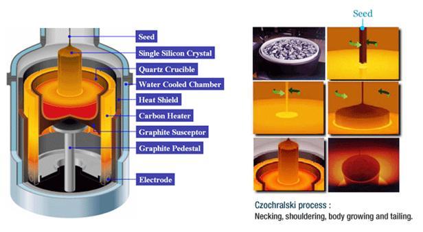
Figure 1.Czochralski crystal growth method (http://melt.snu.ac.kr/research/singlecrystals.php
1-Manijeh Razeghi - The MOCVD Challenge, Second edition, CRC Press, 2011
2-Manijeh Razeghi - Fundamentals of Solid State Engineering, Third Edition, Springer, 2009
3-Manijeh Razeghi - Technology of Quantum Devices, Springer, 2010
10:45 - Lecture by Prof. Eicke R. Weber, Fraunhofer-Institut für Solar Energie System ISE, Germany
Photovoltaics moving into the Terrawatt range: starting the second cycle of PV
|
|
|
|
 |
|
Eicke R. Weber Fraunhofer Institute for Solar Energy Systems ISE and Faculty of Physics and Mathematics, and Faculty of Engineering, Albert-Ludwigs University, Freiburg, Germany |
Innovation and volume production brought about a rapid, unheard-of cost reduction of photovoltaic (PV)technologiesin recent years.Today, PV electricity is cost-competitive with electricity produced by oil-fired power plants, new nuclear power plants and diesel generators. In the last five years, the global production capacity for PV vastly exceeded the market size, fueled by the rapid built-up of PV production in China. The result were prices dropping below the long-term price experience curve, leading to big financial problems for most PV producers worldwide. However, this period is coming to an end in 2016. At a recent workshop last March in Freiburg the start of the second cycle, the second stage of PV was announced, characterized by the need to double production capacity within the next five years from todays ca. 60 GWp/a to 100-120 GWp/a, bringing PV installationsinto the Terawatt range. Scenarios predict for 2030 deployment of several Terawatt of PV power, fueled by a 300-500 GW/a PV market. Today,a window of opportunity exists for new investments in PV production along the whole value chain.
This talk will discuss these developments with focus on the PV technologies expected to dominate the market in the coming years. PV technologies based on crystalline silicon will continue to have the largest market share, drivingdown the price experience curve. In c-Si, there is a whole portfolio of new technologies available that allows cell efficiencies in the 20-25% range to become mainstream, mainly based on the use of n-Si single-crystal wafers. These include PERC-type cells with good backside passivation, hetero-junction cells combining c-Si with a-Si thin film technology, and other advanced cell concepts. However, the largest market share and drivers of the cost curve presently are PV cells based on cast-Si with efficiencies in the 16-18% range. Here, the replacement of expensive Siemens-Si by upgraded metallurgical Si will allow further cost reductions. High-performance multi-crystalline cast Si produced with small seed cyrstals guaranteeing a homogenous grain structure will allow further gains in efficiency.
Module technology is being adapted to be compatible with upcoming cell technologies by introducing new materials and low-temperature interconnection processes. The development is focused on reducing or even avoiding cell-to-module efficiencylosses and achieving a module service life exceeding 30 years, even in challenging climates.Special coatings cut losses due to reflectance and soiling. System performance will improve substantially by the introduction of bifacial modules.
Current thin film technology in the market is primarily based on First Solar’sCdTe-based technology. Encouraging efficiency improvements have been demonstrated. It remains to be seen how much of the thin-film market can be captured by CIGS-type technologies, which have the advantage of high cell efficiencies of small lab-type structures, exceeding 20%, that could not yet be reproduced in large-scale production.
The highest efficiencies are possible in multijunction technology, where the current world record stands at 46%. This can only be used terrestically by employing highly concentrated PV technology, requiring two-achsis tracking, applicapleonly in regions with the highest direct insolation (DNI). Currently, there is currently no major player in the market left over to produce this PV technology on a cost-competitive scale.
Further advancements, like organic or dye-sensitized PV (Graetzel cells), nanostructure-based solar cells, and the exciting developments of Perovskite-based cells are still further from large-scale market introduction. It is questionable if these will ever be cost-competitive with mainstream c-Si based technologies. However, Perovskite-based PV technology might be very interesting as additional layer on c-Si cells, to capture high-energy photons with good efficiency.This might allow to developc-Si cell efficiencies towards the 30% range.
Author contact:
Eicke R. Weber, Fraunhofer ISE, Heidenhofstr. 2, 79100 Freiburg, Germany
Tel.: +49-761-4588-5120, E-Mail: eicke.weber@ise.fraunhofer.de
11:30 - Lecture by Prof. Maurizio Prato, University of Trieste, Italy
Widening our nano-horizons: from organic chemistry to energy to neurosciences
|
|
||
 |
Maurizio Prato Dipartimento di Scienze Chimiche e Farmaceutiche, Università degli Studi di Trieste, Piazzale Europa 1, 34127 Trieste, Italy CIC BiomaGUNE, San Sebastian, Spain |
Nanometer-scale structures represent an intriguing field, where scientists and engineers manipulate materials at the atomic and molecular level to produce innovative materials for making composites and for electronic, sensing, and biomedical applications. Carbon nanomaterials, such as carbon nanotubes, graphene and carbon dots, constitute a relatively young class of materials exhibiting very interesting electronic properties, and are also promising candidates for gas storage and drug delivery.
During this talk, we will show how nanocarbons are particularly suited for a variety of applications, ranging from neurosciences to energy. In particular, we will discuss why carbon nanotubes are ideal materials for integration with nerve tissues. Nanotubes are compatible with neurons, but especially they play a very interesting role in interneuron communication, opening possibilities towards applications in spinal cord repair therapy.
In addition, in combination with catalysts of different nature, carbon nanotube modified surfaces can serve for many scopes. Experiments aiming at the splitting of water to give oxygen, and therefore, molecular hydrogen, ideal for clean energy generation, will be described.
Finally, moving from electrochemical devices to light-driven processes, we will discuss the synthesis and applications of perylene bisimides, which, in combination with polyoxometalates, are ideal partners in the photosplitting of water.
12:15 - Presentation of the Materials for Clean Air Prize - Achilleas Stalios, European Commission