Plenary session

The plenary session is scheduled for Wednesday morning, 17th September (Main Hall) and will consist of a series of outstanding talks.
Three speakers have already confirmed their participation:
- Prof. Claudia Felser, Max Planck Institute for Chemical Physics of Solids, Dresden, Germany - 2025 Czochralski Award Recipient
- Prof. Salvo Coffa, Robert Bosch GmbH, Reutlingen, Germany
- Prof. David A. Muller, School of Applied Physics, Cornell University, USA
It's hard to imagine a richer offering of speakers. And that's the point of the plenary session: provide a shared experience for all conference attendees.
Schedule of plenary session:
09:15 - Introduction - Conference Organizers
09:25 - Welcome address by the Rector of the Warsaw University of Technology
09:30 - Welcome Address by E-MRS President
09:35 - Laudation and Presentation of the Jan Czochralski Award to Prof. Claudia Felser
09:50 - Czochralski Award Laureate - Prof. Claudia Felser, Max Planck Institute Chemical Physics of Solids, Dresden, Germany
 |
||
|
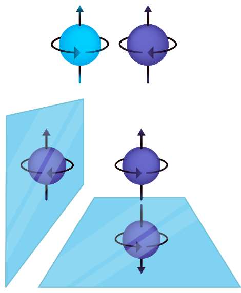
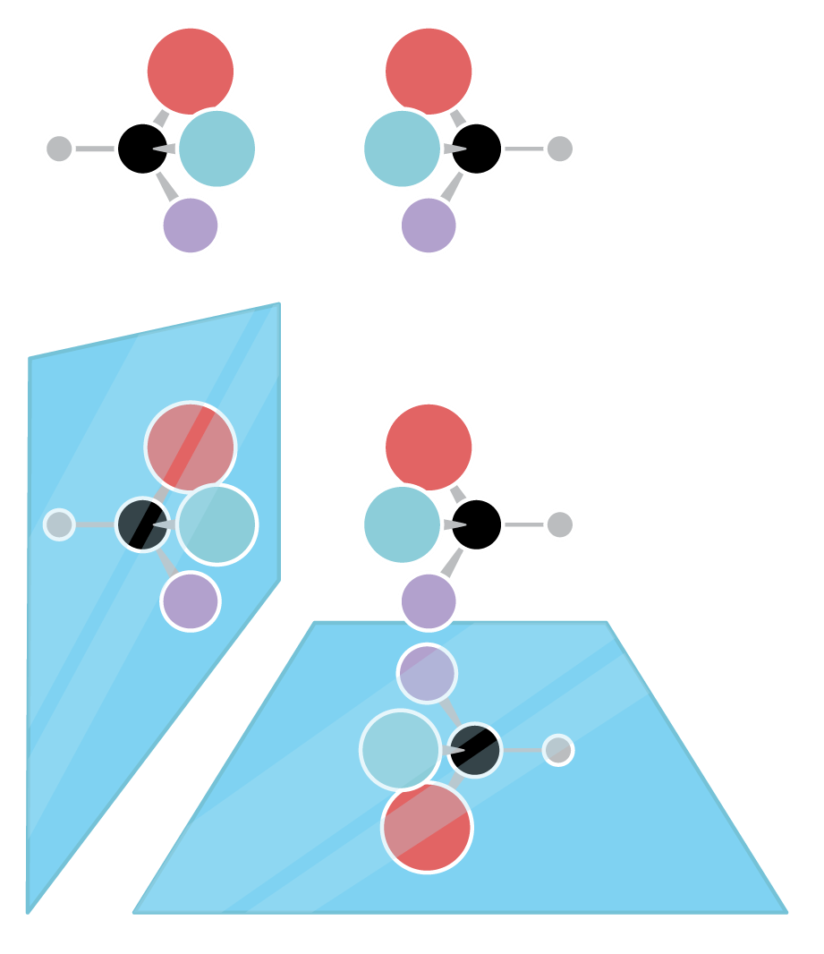
Topology, a well-established concept in mathematics, has nowadays become essential to describe condensed matter. At its core are chiral electron states on the bulk, surfaces and edges of the condensed matter systems, in which spin and momentum of the electrons are locked parallel or anti-parallel to each other. Magnetic and non-magnetic Weyl semimetals, for example, exhibit chiral bulk states that have enabled the realization of predictions from high energy and astrophysics involving the chiral quantum number, such as the chiral anomaly, the mixed axial-gravitational anomaly and axions. The potential for connecting chirality as a quantum number to other chiral phenomena across different areas of science, including the asymmetry of matter and antimatter and the homochirality of life, brings topological materials to the fore.
Chiral electron with spin momentum locked and chiral molecules and their mirror image |
||
 |
 |
10:35 - Prof. Salvo Coffa, Robert Bosch GmbH, Reutlingen - Mobility Electronics Department, Power Semiconductors and Modules
|
The role of material science in power electronics S. Coffa |
||
|
In this talk the importance of new materials introduction in semiconductor processing is highlighted. In particular, cases in which materials science innovation have been combined with proper industrial exploration of the new materials properties will be discussed. As known, performances of power devices are of paramount importance in energy consumption reduction in many practical applications. The roadmaps of modern power devices is driven by three major development pillars; a) novel elementary cell structure; b) advanced interconnects; c) use of different semiconductor materials (moving from Si to SiC and GaN). Improvements in any of these pillars are strongly driven by new materials introduction. The focus of the presentation is to show how the introduction of SiC and GaN with their superior electronic and thermal properties (and in spite of problems linked to defects and higher costs compared to Si) has revolutionized the field of power devices. Today semiconductor companies are heavily using SiC and GaN in the production of power devices. This has been made possible by the huge work of the material science community (improvement in crystal growth, epitaxy, defect reduction and screening, use of ion implantation on compound semiconductor, etc). Finally, it will be shown that the lower defect density, the larger availability, the possibility to use large area substrates and the overall reduction in costs achieved for SiC, is offering the possibility to use the material for other applications (SiC integrated photonics, quantum computing and others still to come) |
||
11:20 - Prof. David A. Muller, School of Applied Physics, Cornell University, USA
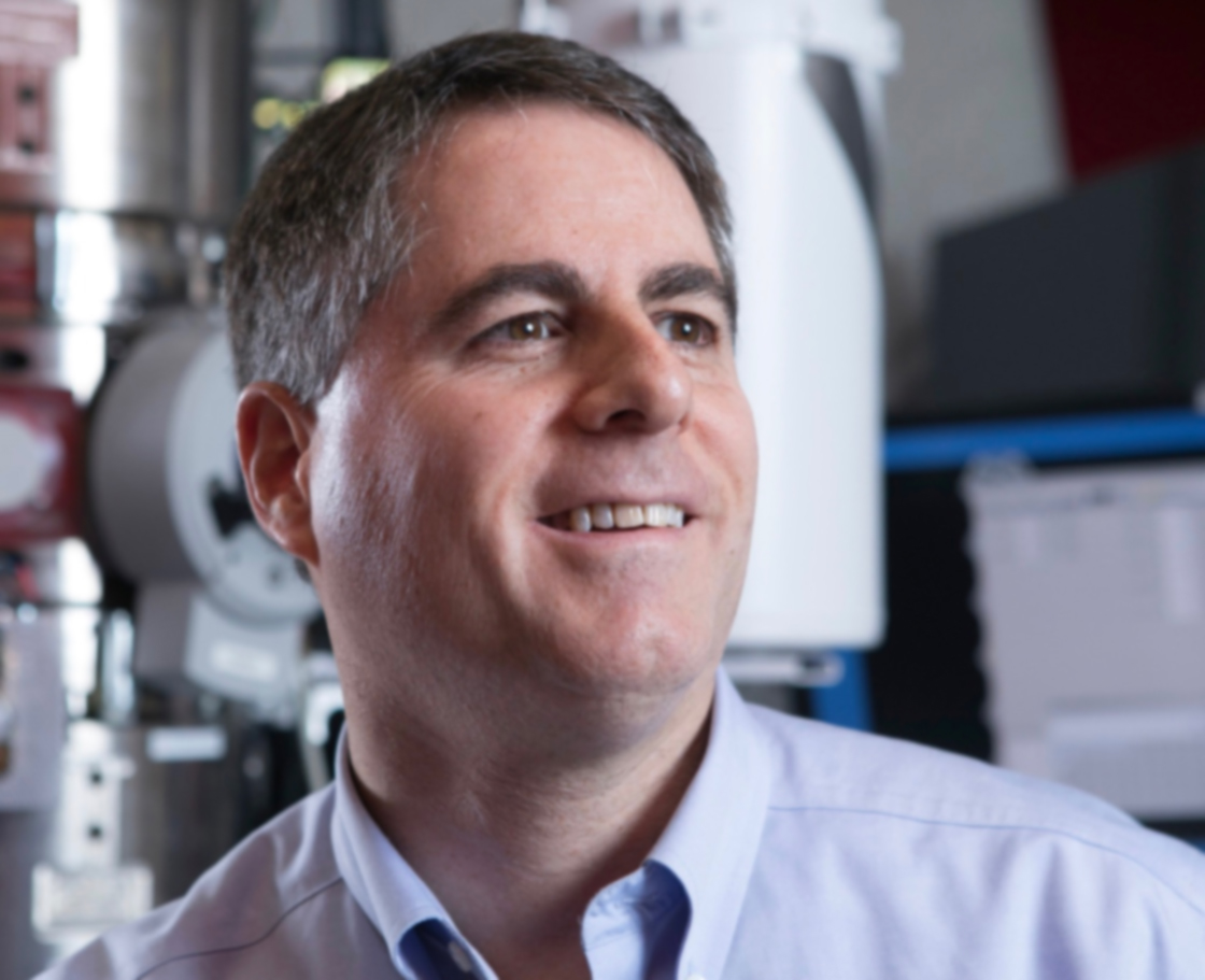 |
David A Muller
|
|
|
With recent advances in detector technology and ptychographic phase-retrieval algorithms to unscramble multiple scattering, the resolution of the electron microscope is now limited only by the dose applied to the sample, and thermal vibrations of the atoms themselves. At high doses, these approaches have allowed us to image the detailed vibrational envelopes of individual atom columns as well as locating individual interstitial atoms. The three-dimensional nature of the reconstruction means surface relaxations can be distinguished from the bulk structure, and atomic-scale interface roughness and step edges inside devices can be resolved – including gate-all-around transistors and Josephson junctions. Even the location of all atoms in thin amorphous films now seems within reach. The reduced sensitivity to chromatic aberrations also makes these ptychographic-like approaches of interest for thick biological or polymer samples or operando liquid-cell experiments, where we have been able to demonstrate a fivefold improvement in dose efficiency over conventional cryo-EM. |
||
12:05: PCAM - GPB (Gian Paolo Brivio) Award by Prof. Horst-Günter Rubahn
Polish Academy of Sciences Al. Lotnikow 32/46 02-668 Warsaw POLAND
4822 8436601 x 31654822 8430926
mycie@ifpan.edu.pl
Warburger Str. 100, A4.226, 33098 Paderborn, Germany
lindner@physik.upb.deStrada Ottava 5 Z.I., 95121 Catania, Italy
rosariaanna.puglisi@cnr.itDepartment of Materials Science and Engineering - South Korea
sangouk.kim@kaist.ac.kr