Tutorial
Vapor-Phase Thin-Film Synthesis: fundamentals, design, and applications
Room Cassin (Ground floor)
General description
The tutorial aims at providing an overview of: (i) thin-film vapor-based synthesis techniques, (ii) fundamental atomic-scale processes and phenomena encountered during vapor-based film deposition, (iii) theoretical and computational tools used for thin-film design, and (iv) applications of nanoengineered thin films and coatings with a focus on nanomechanical characterization and stress evolution. The primary audience of the tutorial is Ph.D. and M.Sc. students working in the field, but also scientists and engineers. Lectures will be given by the organizers of the Symposium B “Nano-engineered coatings and thin films: from design to applications” but also by experts in the field, as detailed in the following.
Schedule and modules
|
Sunday, May 24 |
Stress generation and evolution during thin film growth |
Gregory Abadias University of Poitiers |
|
Sunday, May 24 |
Mechanical characterization of thin films and interfaces |
Barbara Putz EMPA Thun |
|
Monday, May 25 |
Thin film nucleation and growth |
Kostas Sarakinos University of Helsinki, Finland |
|
Monday, May 25 |
Computational tools for designing thin films |
David Holec Montanuniversität Leoben |
|
Tuesday, May 26 |
Physical vapor deposition and reactive sputtering |
Tomas Kubart, Uppsala University |
|
Tuesday, May 26 |
Chemical vapor deposition |
Panos Patsalas Thessaloniki University, Greece |
Registration closed
Module description
1. Physical vapor deposition and reactive sputtering
Physical vapour deposition (PVD) techniques are widely used for synthesis of various thin films from laboratory to industrial scale. This module aims at understanding of the principles underlying various PVD methods and emphasizes the relation between processing conditions and the resulting film properties. Particular attention is devoted to plasma-based techniques.
The module will cover following topics: Introduction to PVD -definition, mechanisms of vapour generation (evaporation and sputtering), and particle energies; Role of plasmas in PVD and ion-assistance; Magnetron sputtering and principles of reactive sputter deposition. To illustrate key physical processes, examples including low temperature synthesis of photocatalytic materials, achieving high deposition rate of compound films, and the growth of transparent conducting oxides are discussed.
2. Chemical vapor deposition
Chemical methods for synthesis of nanoengineered films and coatings, such as chemical vapor deposition (CVD), plasma-enhanced CVD (PECVD), and atomic layer deposition (ALD), are in the forefront of the thin film science and technology, due to their potential of accurate control of the film chemistry, process scalability, and cost effectiveness. In this module, an introduction to these techniques will be presented; it will include the basic principles, reactor design considerations, reactor optimization, and the role of kinetics on the film microstructure. A review of the nanoengineered films and coatings grown by these techniques, with emphasis to metal nitrides, will be provided. The formation of multicomponent nitride films and coatings by these techniques will be considered, and the factors that are used to produce nanocomposites or ternary and quaternary nitride alloys will be critically evaluated. Finally, a critical comparison with the corresponding PVD films and coatings in view of the potential industrial applications will conclude the module.
3. Thin film nucleation and growth
Thin-film technology is pervasive in many applications, including microelectronics, optics, magnetics, hard and corrosion resistant coatings, micromechanics, etc. Progress in each of these areas depends upon the ability to selectively and controllably deposit thin films (thickness ranging from tens of angstroms to micrometers) with specified physical properties. This, in turn, requires control – often at the atomic level – of film microstructure and microchemistry. In this module, the fundamental mechanisms that control vapor condensation, atomic diffusion, island nucleation and growth, island coalescence and coarsening, and continuous film formation will be described briefly discussed. Experimental results and simulation data related to growth in homoepitaxial systems, as well as to growth in polycrystalline weakly-interacting film/substrate systems, will be used as illustrative examples. The effect of energetic bombardment on film microstructural evolution will also be highlighted.
4. Stress generation and evolution during film growth
The presence of stress in thin films and functional coatings constitutes a major concern in many technological applications, as excessive residual stress levels can dramatically affect the performance, reliability, and durability of material components and devices. This module will start with a description of residual stress sources in PVD thin films, with focus placed on intrinsic stress. Stress evolutions during film growth will be presented, and the underlying atomistic and microscopic mechanisms will be discussed in the framework of existing analytical models. Experimental methods for measuring stress in thin films will be reviewed, with main emphasis on wafer-curvature. The influence of growth conditions on intrinsic stress, such as kinetics (substrate temperature and deposition flux), energetics (working pressure, bias voltage) will be addressed together with the role of impurities and alloying effects. Finally, strategies to control and mitigate stress for specific applications will be proposed.
5. Mechanical characterization of thin films and interfaces
The tutorial on thin film and interface mechanics provides an essential overview of how mechanical principles apply to materials on a micro- and nanoscale, where size-, surface- and interface- effects become dominant. This module starts with explaining the unique challenges and behaviors of materials where thickness is minimal compared to other dimensions. The specialized experimental techniques for evaluating material and interface properties will be introduced and compared, including nanoindentation and other micro-mechanical testing methods such as microbeam bending, microtensile testing, and bulge testing. A specific focus will be put on interface mechanics, providing a focused overview of the physical principles and behaviors governing the boundary regions where two different materials meet. These interfaces play a critical role in determining the overall function and reliability of layered structures and thin film devices. After introducing the fundamental principles and core concepts such as adhesion theory, interfacial energy, and the mechanics of interfacial fracture, benefits and limits of different qualitative and quantitative techniques for measuring adhesion energy will be reviewed and discussed. Finally, strategies to control and promote interface adhesion for specific applications will be proposed
6. Computational tools for designing thin films
Modelling represents an important part of materials science. On the one hand, it allows to reduce experimental efforts by accurate pre-screening (optimisation of composition, sample design, testing conditions). On the other hand, modelling can provide insights beyond the experimental capabilities (resolution in space and time, separating various effects etc.). In this tutorial, we will endeavour on a journey over several length-scales, and review modelling techniques spanning from continuum mechanics, over classical thermodynamics and phase-field modelling to atomistic approaches (Monte Carlo and molecular dynamics) and ab initio methods based on Density Functional Theory. For each technique we will briefly discuss its underlying principles, typical applications (with a special focus on thin films), advantages and limitations. The tutorial aims additionally on demonstrating, how problems formulated in “experimentalist language” can be translated into a model and vice-versa
Lecturers
|
|
Gregory Abadias is Professor at the Physics Department of the University of Poitiers, and Deputy Director of the Department of Physics and Mechanics of Materials, at CNRS Pprime Institute, France. He received his Ph.D. degree in materials science in 1998 at National Polytechnic Institute of Grenoble (INPG), and he is currently group leader of thin films activities at Pprime Institute. His current research interests focus on the understanding of thin film growth dynamics using real-time and in situ diagnostics as well as computational modelling, with main emphasis on growth |
|
| manipulation strategies to control morphology and stress development in sputter-deposited metallic layers, including compositionally complex alloys. He has co-authored more than 160 papers in peer-review journals and one book chapter on stress in PVD thin films. He was the French representative of the Surface Engineering Division of IUVSTA for 2022-25 triennium. He serves as Editor of Surface and Coatings Technology journal since 2016. | ||

 |
David Holec is a group leader of Computational Materials Science at the Department of Materials Science, Montanuniversität Leoben. David received his MSc degree in Condensed Matter Physics from Masaryk University, Brno, Czech Republic, in 2005, and PhD degree in Materials Science from Cambridge University, UK, in 2008. Since 2008, he has been conducting research in the area of electronic structure and atomistic modelling of thin films, structural alloys as well as functional low-dimensional materials at the Montanuniversität Leoben. Since 2013 he is also a guest researcher at |
|
| TU Wien, and has served as guest researcher at several research institutions (RWTH Aachen, DE, CSU Changsha, CN).His research interests span from nitride and oxide protective coatings, over novel semiconductors, intermetallic alloys, shape memory materials, steels to and carbon nanostructures, methane pyrolysis and hydrogen storage. He has published over 200 peer-reviewed papers and has presented 20 invited talks at international conferences. Since 2024, he serves as an editor of Results in Surfaces and Interfaces. He has supervised a number of BSc, MSc, and PhD students. He teaches several courses on materials modelling and solid-state physics. | ||
 |
Tomas Kubart is an Associate Professor at the Department of Solid-State Electronics at Uppsala University. He leads the Thin Films group and is responsible for the Materials synthesis area at Myfab Uppsala, the local node of the national research infrastructure for micro- and nanofabrication. His research focuses on highly ionized deposition techniques and the development of novel methods for producing high-quality thin films, especially oxides, for electronics and energy applications. |
|
 |
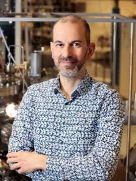
Panos Patsalas is Professor of Advanced Materials in the Department of Applied and Environmental Physics of Aristotle University of Thessaloniki (AUTH) and Director of Studies of the Post-graduate (MSc) course on Nanoscience and Nanotechnology provided jointly by the Faculties of Physics, Chemistry and Medicine. He is a graduate of the Faculty of Physics of the University of Ioannina and holds a PhD in Physics from AUTH. He has served as the Director of the Department of Applied and Environmental Physics at AUTH. For more than fifteen years he has been a member of the Board of Delegates of the European Materials Research Society for which he |
|
| periodically organizes international symposia and tutorials in Strasbourg. His research focuses on the synthesis of advanced materials for applications in photonics and biomedical technology in collaboration with an extensive network of universities and research institutions in Greece, UK, USA, France, and Israel. He has participated and/or coordinated several research projects, supervised 11 PhD theses (8 completed) and has been advisor (secondary supervisor) of dozens of other PhDs in the Faculties of Physics and Chemistry of AUTH and Materials, Physics and Medicine of the University of Ioannina. He has organized 14 international conferences, given >50 invited talks abroad, published >180 publications in international peer-reviewed journals. | ||
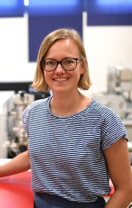 |
Barbara Putz is Group Leader at the Laboratory of Mechanics of Materials and Nanostructures at Empa in Thun and Assistant Professor at the Department of Materials Science at Technical University of Leoben. She received her PhD in Materials Science from Technical University of Leoben in 2017. Her research interests include the deformation behaviour of nanocomposite and nanolaminate films grown by vapor techniques and novel techniques for high quality interface engineering for different material combinations. In 2024, she received an ERC Starting grant for developing programmable interfaces |
|
| towards reliable and recyclable composite materials via debonding on demand. She also teaches several courses on Materials Science basics at the BSc and MSc level. | ||
 |
Kostas Sarakinos is Professor at the Department of Physics at the University of Helsinki, Finland, and Guest Researcher at the Royal Institute of Technology (KTH) in Stockholm, Sweden. Kostas’s research interests include atomistic processes during film nucleation and growth, growth manipulation, in situ growth monitoring, and deterministic and stochastic film growth simulations. He has co-authored 80 papers, 4 book chapters, and 1 book. He teaches courses related to materials, surface, and thin-film physics at undergraduate and post-graduate level. |