PETMEM Workshop 2019: PiezoElectronic Transduction devices
![]()
WORKSHOP OPEN TO ALL PARTICIPANTS on Friday May 31 from 8:30 to 13:00
Room Med 3 - level 1
PETMEM is a Horizon 2020 project concerned with resolving a stumbling block key to further advancements in computing. Critically computer clock speeds have not significantly increased since 2003, creating a challenge to invent a successor to CMOS technologies able to resume the improvement in clock speed and power performance. The key requirements for a viable alternative are scalability to nanoscale dimensions – following Moore’s Law – and simultaneous reduction of line voltage in order to limit switching power. Achieving these two aims for both transistors and memory allows clock speeds to again increase with dimensional scaling, a result that would have great impact across the IT industry.
The PETMEM Consortium comprises 11 international partners: Bio Nano Consulting (London UK), IBM Research (Zurich, Switzerland), Max Planck Institute (Dresden and Halle, Germany), Solmates (Enschede, The Netherlands), SINTEF (Oslo, Norway), National Physical Laboratory (Teddington, UK), University of Gent (Gent, Belgium), AixAcct (Aachen, Germany), ElectroSciences (Surrey, UK) and DCA (Turku, Finland).
Towards the development of new transistor technologies, our project has made advancements in a variety of fields. From piezoelectric and dielectric deposition, processing and characterisation to development of a little known class of materials known as piezoresistive materials has been extensively explored with advances in 2D materials and lanthanide materials yielding new insights and technological avenues of exploration. It is our intention to communicate these developments to the academic community with the intention of exploring new collaborations and scientific relationships.
Program
08.30 - 09.00: Tea & Coffee / Networking
09.00 - 09.20: Introduction to PETMEM | Dr Nicholas P. Chadwick (BNC)
09.20 - 10.30: PETMEM Technological Achievements (Tools and Processes)
09.20 - 09.30: DCA – Advances in Deposition Tool – Dr Nils Hoffman
09.30 - 09.50: Solmates/Sintef – Piezoelectric Materials, Applications and Commercialization – Dr Matthijn Dekkers / Dr Frode Tyholdt
09.50 - 10.10: University of Gent / Max Planck Institute – Piezoresistive Material, Applications and Advances – Prof Philippe Smet / Dr Amilcar Bedoya Pinto
10.10 - 10.30: AixAcct – Metrology Tool Development – Mr Lutz Nielen
10.30 - 11.00: Tea & Coffee / Networking
11.00 - 11.45: PETMEM Device and Results
11.00 - 11.15: National Physical Laboratory – Advanced Modelling of PET Devices – Dr Ivan Rungger
11.15 - 11.45: IBM Zurich/EMPA - PET Device fabrication and Processing – Mr Youri Popoff
11:45 - 12:15: External Speaker - Professor Dennis Newns - Pimpernel, Science, Software and Information Technology
12.15 - 12.30: PETMEM Outlook | Dr Jean Fompeyrine (IBM Zurich)
12.30 - 13:00: Discussion/ Networking/ Tea & Coffee
13.00: Close of Session
About the PETMEM project
Computer clock speeds have not significantly increased since 2003, creating a challenge to invent a successor to CMOS technology able to resume the improvement in clock speed and power performance. The key requirements for a viable alternative are scalability to nanoscale dimensions – following Moore’s Law – and simultaneous reduction of line voltage in order to limit switching power. Achieving these two aims for both transistors and memory allows clock speed to again increase with dimensional scaling, a result that would have great impact across the IT industry. PETMEM is a European partnership amongst Universities, Research Institutions, SMEs and a large company that will focus on the development of new materials and characterization tools to enable the fabrication of an entirely new low-voltage memory element. This element makes use of internal transduction in which a voltage state external to the device is converted to an internal acoustic signal that drives an insulator-metal transition.
Modelling based on the properties of known materials at device dimensions on the 15nm scale predicts that this mechanism enables device operation at voltages an order of magnitude lower than CMOS technology (power is reduced two orders) while achieving 10GHz operating speed. Additional, possibly earlier development applications include ultralow power RF switches for telecommunications devices and low voltage several GHz logic devices especially for portable equipment.
|
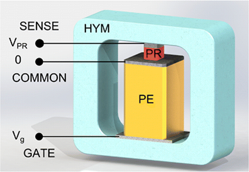
The principle behind the piezoelectric transistor. A voltage driven piezoelectric element creates high stresses in a piezoresistive element changing its electrical resistance from an insulator to a conductor. |
PETMEM partners
The consortium that will develop PETMEM technologies comprises 11 partners: Bio Nano Consulting (London UK), IBM Research (Zurich, Switzerland), Max Planck Institute (Dresden and Halle, Germany), Solmates (Enschede, The Netherlands), SINTEF (Oslo, Norway), National Physical Laboratory (Teddington UK), University of Gent (Gent, Belgium), EMPA (Switzerland), Aixacct (Aachen Germany), Electrosciences (Surrey, UK), EMPA (Dübendorf, Switzerland) and DCA (Turku, Finland).
For more information contact the consortium at: www.petmem.eu
Scopes
- Advance modelling of piezo-devices
- Piezoelectric materials
- Piezoresistive materials
- Piezo-material characterization and metrology
- Tools development for the piezo industry
- Processes for piezo-device fabrication
- Novel application of the PET technology
Contact
Dr Abiola Oladipo, (Bio Nano Consulting Ltd, UK): abiola.oladipo@bio-nano-consulting.com
This project has received funding from the European Union’s Horizon 2020 research and innovation programme under grant agreement No 688282.